
An outside view on your board before you release it to manufacturing. An error found on the schematic costs an hour; the same error found on a prototype costs a new batch of boards and several weeks.
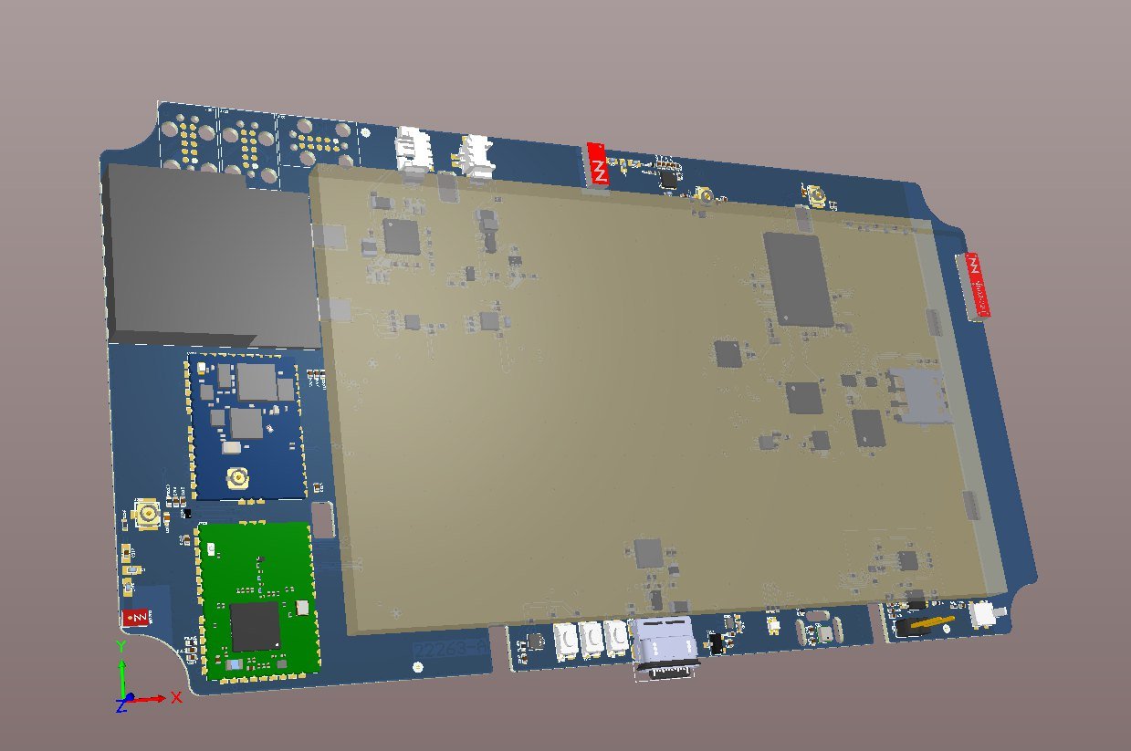
Schematic, layout (Altium, KiCad or Gerbers) and BOM, with a short description of what the board does.
A complete, point-by-point review by an EPFL-trained electronics engineer.
Every finding is ranked by priority, with the proposed fix. We can then go through it together.
The schematic as PDF or source files, the layout (Altium or KiCad project, or Gerber files), the BOM and, if possible, a short description of what the board does.
From about CHF 900 for a typical board. The price depends on layer and component count, and it is confirmed before we start. Our quote tool gives you an estimate in two minutes.
Yes. We work in Altium Designer, but we can review boards designed in KiCad, EasyEDA or other tools, from the source files or the Gerbers.
You can fix it yourself from the report, or hand the rework over to us. See our electronics design office in Lausanne.