
Example with a study case using COMSOL AC/DC (source: comsol.com paper on modeling PCB-based inductive position sensors with the COMSOL AC/DC module).
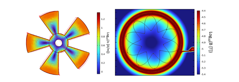
Figure 1. Target surface current distribution and coil-plane magnetic field distribution.
Context
In a perfect world without mechanical or physical interferences, inductive position sensors (IPS) would operate with minimal error. However, real-world applications always involve non-ideal conditions. Various factors such as additional metallic parts, feeding wires, multilayer PCB designs and nearby ground planes can introduce accuracy errors. Evaluating and optimizing these factors is essential for accurate IPS performance.
This study focuses on three key factors affecting IPS accuracy using COMSOL simulations:
- Number of PCB layers (2 vs. 4)
- Feeding wires connecting Rx coils to the IC
- Nearby metallic ground planes
Methodology
Starting from an ideal configuration, non-idealities are progressively introduced. The following protocol determines the accuracy for each configuration:
- Simulations: perform simulations with different air gaps between coils and target, recording the Rx signal amplitude.
- Angle calculation: calculate the sensor's angle using Clarke's transformation on the Rx signals followed by an arctangent calculation.
- Accuracy assessment: compare the calculated angle with the target's reference position.
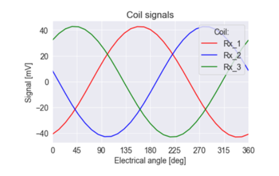
Figure 2. Simulated Rx coil signal amplitude vs. target position over one full electrical period.
Results
1. Ideal case: 4-layer PCB. An ideal 4-layer PCB with 0.3 mm spacing between planes shows nearly perfect accuracy across various air gaps.
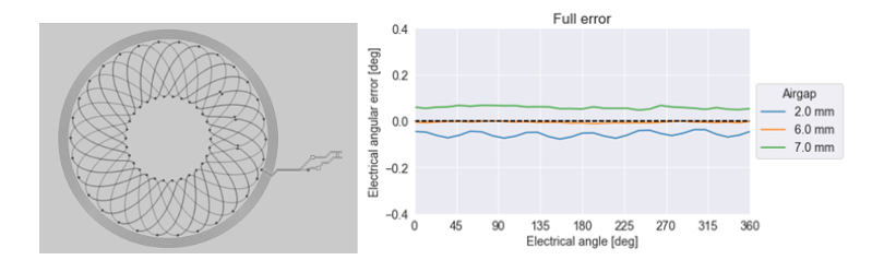
Figure 3. PCB design of an IPS in an ideal case, 4 layers, and the associated accuracy.
2. Introducing a ground plane. Adding a metallic ground plane introduces a first-harmonic error, increasing with the ground plane's proximity to the coils.
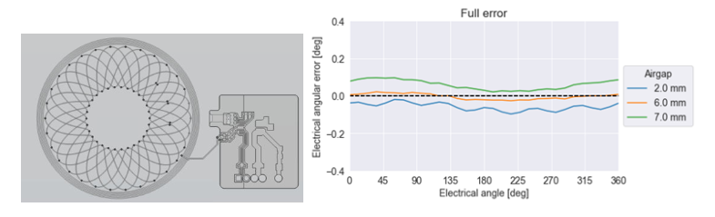
Figure 4. PCB design including a ground plane, 4 layers, and the associated accuracy.
3. Feeding-wire configuration. Feeding wires introduce parasitic surfaces. Two configurations are tested, 60 deg and 120 deg electrical separation.
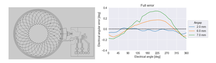
Figure 5. 60 deg electrical feeding configuration, 4 layers, and its accuracy.
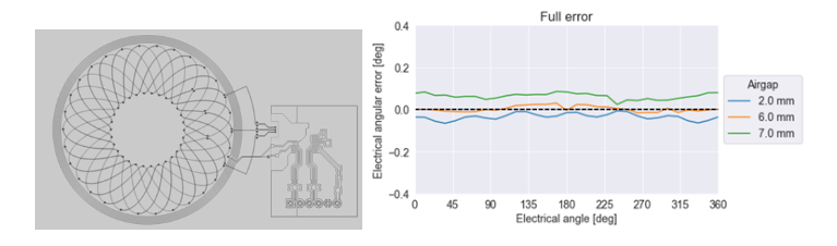
Figure 6. 120 deg electrical feeding configuration, 4 layers, and its accuracy. The 120 deg separation demonstrates superior accuracy.
4. 2-layer PCB configurations. For 2-layer PCBs with 1.6 mm spacing:
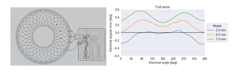
Figure 7. 60 deg electrical feeding configuration, 2 layers, and its accuracy.
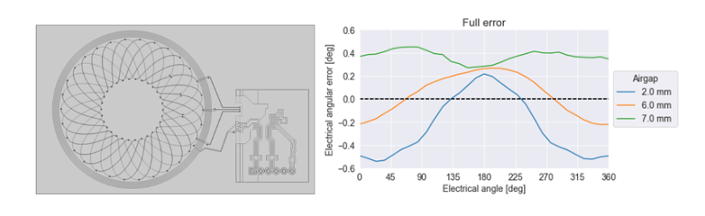
Figure 8. 120 deg electrical feeding configuration, 2 layers, and its accuracy. Both 2-layer configurations show significant errors due to larger horizontal parasitic surfaces from feeding lines, which are minimized in the 4-layer design.
Conclusion
Optimizing PCB design, especially the number of layers and the arrangement of feeding wires, is vital for minimizing accuracy errors in inductive position sensors. This study underscores the importance of careful PCB layout to ensure high-performance sensor operation in real-world applications.